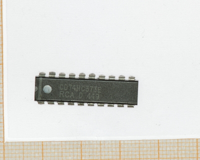
 CD74HC373E
2-V to 6-V VCC Operation
Wide Operating Temperature Range of
–55°C to 125°C
Balanced Propagation Delays and
Transition Times
Standard Outputs Drive up to 15 LS-TTL
Loads
Significant Power Reduction Compared to
LS-TTL Logic ICs
1438
CD74HC373E
2-V to 6-V VCC Operation
Wide Operating Temperature Range of
–55°C to 125°C
Balanced Propagation Delays and
Transition Times
Standard Outputs Drive up to 15 LS-TTL
Loads
Significant Power Reduction Compared to
LS-TTL Logic ICs
1438
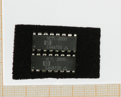 HCTL-2000
• Interfaces Encoder to
Microprocessor
• 14 MHz Clock Operation
• Full 4X Decode
• High Noise Immunity:
Schmitt Trigger Inputs Digital
Noise Filter
• 12 or 16-Bit Binary Up/
Down Counter
• Latched Outputs
• 8-Bit Tristate Interface
• 8, 12, or 16-Bit Operating
Modes
• Quadrature Decoder Output
Signals, Up/Down and Count
• Cascade Output Signals, Up/
Down and Count
• Substantially Reduced
System Software
1424
HCTL-2000
• Interfaces Encoder to
Microprocessor
• 14 MHz Clock Operation
• Full 4X Decode
• High Noise Immunity:
Schmitt Trigger Inputs Digital
Noise Filter
• 12 or 16-Bit Binary Up/
Down Counter
• Latched Outputs
• 8-Bit Tristate Interface
• 8, 12, or 16-Bit Operating
Modes
• Quadrature Decoder Output
Signals, Up/Down and Count
• Cascade Output Signals, Up/
Down and Count
• Substantially Reduced
System Software
1424
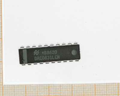 DAC0831LCN
8-bit Accuracy DAC
Easily Interfaces to Most Microcontrollers
Double-Buffered, Single Buffered or Flow Through Options
Linearity Specified with Zero and Full Scale Adjust
Operates Stand-Alone
1428
DAC0831LCN
8-bit Accuracy DAC
Easily Interfaces to Most Microcontrollers
Double-Buffered, Single Buffered or Flow Through Options
Linearity Specified with Zero and Full Scale Adjust
Operates Stand-Alone
1428
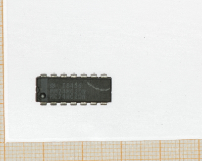 DM74LS74A
This device contains two independent
positive-edge-triggered D flip-flops with complementary outputs. The information on the D input is accepted by the flip-flops on the positive going edge of the clock pulse. The
triggering occurs at a voltage level and is not directly related to the transition time of the rising edge of the clock. The data on the D input may be changed while the clock is low or high
without affecting the outputs as long as the data setup and hold times are not violated. A low logic level on the preset or clear inputs will set or reset the outputs regardless of the logic levels of the other inputs.
1425
DM74LS74A
This device contains two independent
positive-edge-triggered D flip-flops with complementary outputs. The information on the D input is accepted by the flip-flops on the positive going edge of the clock pulse. The
triggering occurs at a voltage level and is not directly related to the transition time of the rising edge of the clock. The data on the D input may be changed while the clock is low or high
without affecting the outputs as long as the data setup and hold times are not violated. A low logic level on the preset or clear inputs will set or reset the outputs regardless of the logic levels of the other inputs.
1425
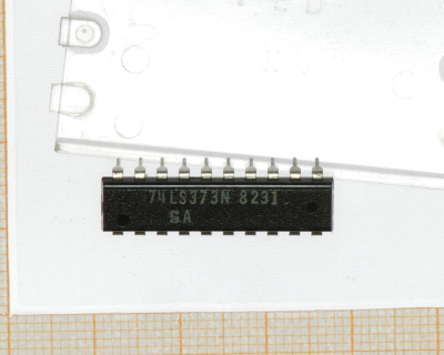 SN74LS373N
Choice of Eight Latches or Eight D-Type
Flip-Flops in a Single Package
3-State Bus-Driving Outputs
Full Parallel Access for Loading
Buffered Control Inputs
Clock-Enable Input Has Hysteresis to
Improve Noise Rejection (’S373 and ’S374)
P-N-P Inputs Reduce DC Loading on Data
Lines (’S373 and ’S374)
1439
SN74LS373N
Choice of Eight Latches or Eight D-Type
Flip-Flops in a Single Package
3-State Bus-Driving Outputs
Full Parallel Access for Loading
Buffered Control Inputs
Clock-Enable Input Has Hysteresis to
Improve Noise Rejection (’S373 and ’S374)
P-N-P Inputs Reduce DC Loading on Data
Lines (’S373 and ’S374)
1439